


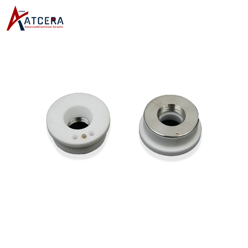
Substrate in electronic products plays the function of structural support, electrical connectivity and heat dissipation, ceramic substrate has excellent insulation and thermal conductivity properties, which make it more and more widely used in the integrated circuit and semiconductor industry, especially for high power density components like LED、LD、IGBT、CPV, etc. Electrical connectivity function needs to be realized through ceramic substrate metallization, which is also a critical process of ceramic substrate application.
Material for ceramic substrate metallization can be copper, nickel, silver, aluminum, tungsten, molybdenum, etc. According to the manufacture process, metallized ceramic substrates are generally classified as thick printing ceramic substrate (TPC), thin film ceramic substrate (TFC), direct bonded copper ceramic substrate (DBC), direct plated copper ceramic substrate (DPC), active metal brazed ceramic substrate (AMB), laser activating metallilzed ceramic substrate (LAM), etc. In addition, there are high temperature co-firing and low temperature co-firing methods to fabricate metallized ceramic substrates (HTCC and LTCC), which are widely used for multilayer metallized substrates. It is necessary to choose the appropriate metal material, metal layer thickness and metallization process according to application.
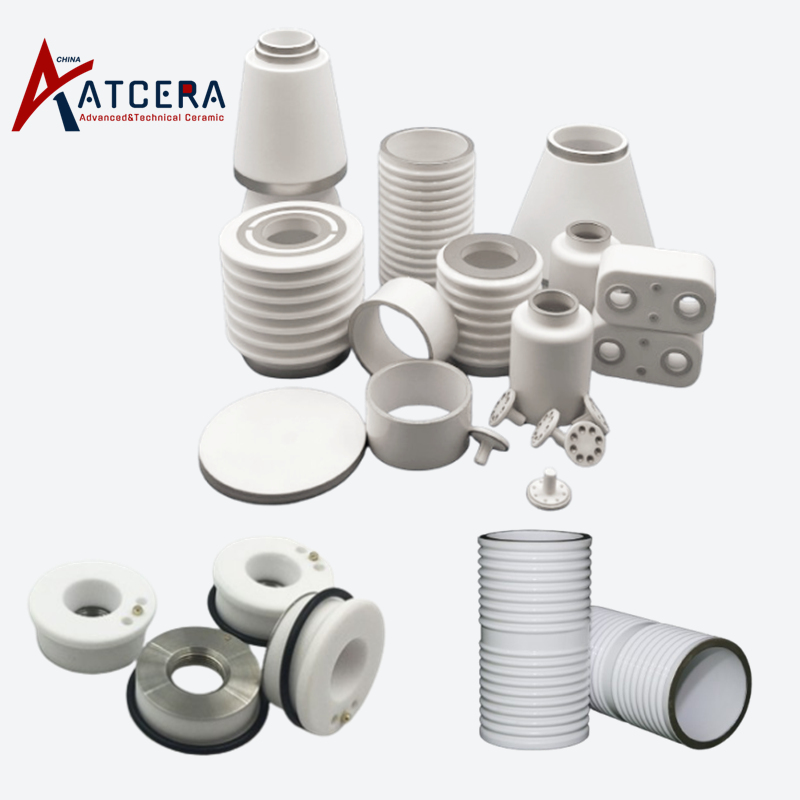
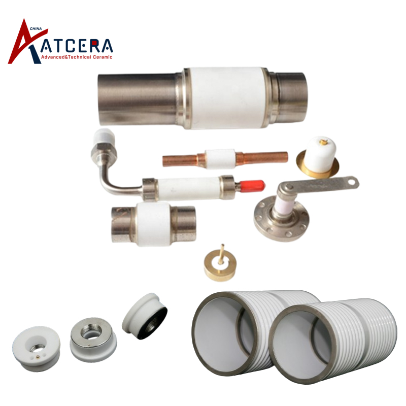
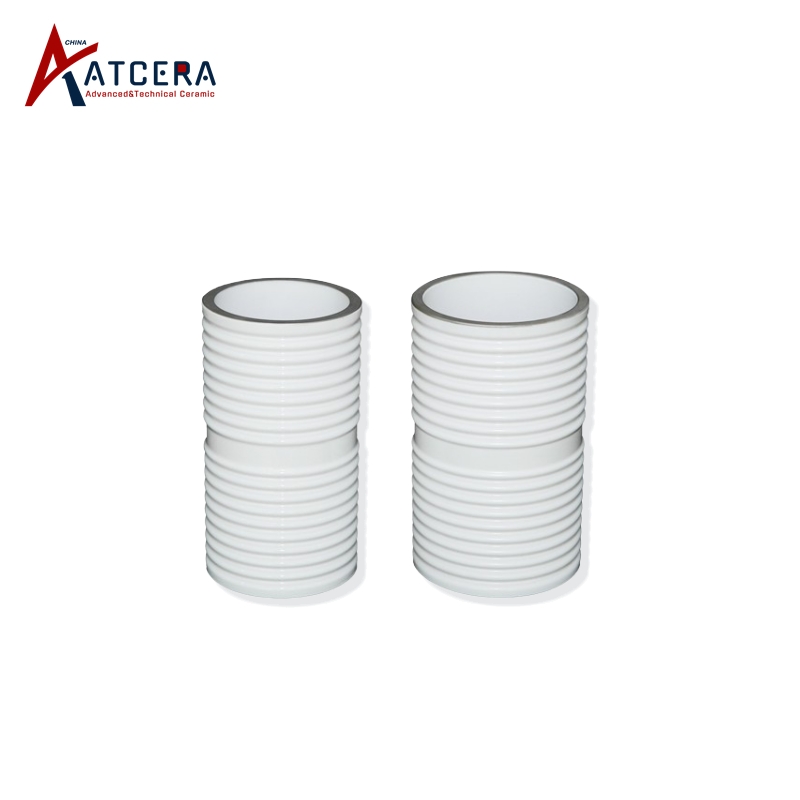
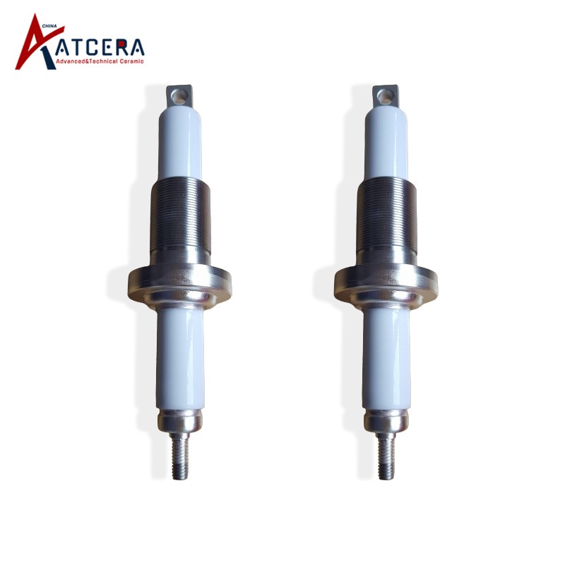
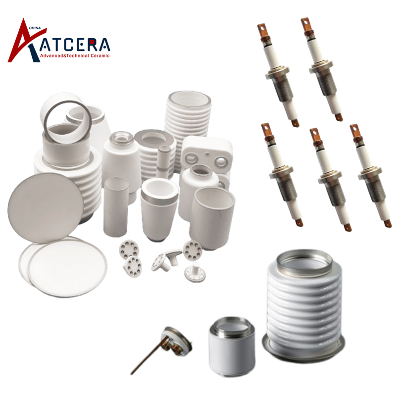
| view all metalized ceramic products |

 According to your application scenario, analyze the needs, choose the appropriate material and processing plan.
 Professional team, quick response, can provide solutions and quotations within 24 hours after confirming the demand.
 Flexible business cooperation mechanism, support at least one piece of quantity customization.
 Quickly provide samples and test reports to confirm that the product meets your needs.
 Provide product use and maintenance suggestions to reduce your cost of use.


