Aluminum nitride ceramics, as an excellent heat dissipating substrate material, has attracted much attention in the field of electronic packaging due to its excellent thermal conductivity. However, the natural defect of this material is its non-conductivity, which directly limits its direct application in the heat dissipation substrate of high-power electronic devices. Therefore, the surface metallization of aluminum nitride ceramic substrate to give it electrical conductivity has become one of the key technologies to promote its wide application.
The core of the metallization process is to ensure that the metal can effectively wet the ceramic surface at high temperatures, thus forming a solid metal-ceramic interface. The strength of this binding force is directly related to the stability and reliability of the package structure, and is a key index to evaluate the success of metallization. In view of this, the metallization technology of aluminum nitride ceramics not only needs to overcome the wettability challenge caused by the strong covalent bonding properties of aluminum nitride ceramics, but also needs to ensure the formation of a strong and uniform bond between the metal layer and the ceramic matrix.
At present, the technical path of aluminum nitride ceramic metallization mainly focuses on the following aspects:
(The other three ways to metallize aluminum nitride ceramic substrates can be check in a previous article: Challenge of Aluminum Nitride Substrate Metallization Technology)
Thin Film Method (TFC)
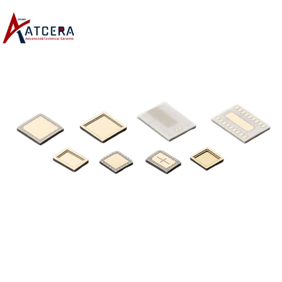
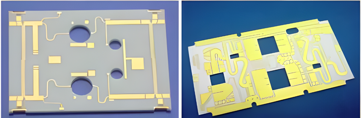
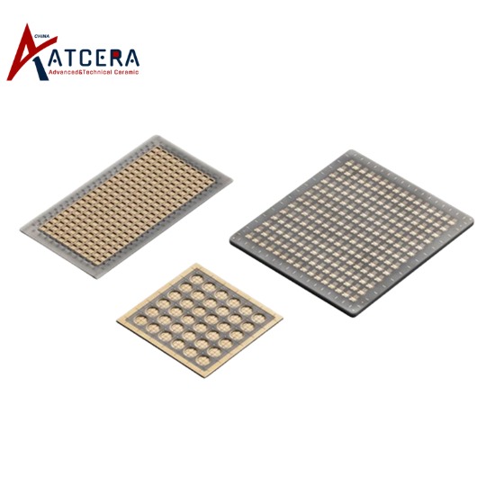
Thin film method refers to the technology of directly depositing metal layer on the surface of AlN substrate by sputtering process, and then preparing the metal layer pattern into a circuit by means of evaporation, lithography and etching. The film not only refers to the actual thickness of the film, but also refers to the way the film is produced on the substrate. Thick film technology is an addition technology, and thin film technology is a subtraction technology. The use of photolithography and etching processes to make the film technology to obtain a smaller graphic feature size, clearer lines, more suitable for high density and high frequency environment, but directly on the surface of the ceramic substrate metallized metal layer adhesion is not high, and aluminum nitride substrate and metal thermal expansion coefficient does not match, will be subjected to greater thermal stress in the work. In order to improve the adhesion of metallized layer and reduce the thermal stress between ceramic and metal, ceramic substrate generally adopts multi-layer metal structure.
Direct Copper Plating (DPC)
Direct copper plating method is to use semiconductor technology to sputter copper seed layer on the ceramic substrate, and then through exposure, development, film removal and other photolithography process to achieve the line pattern, and finally through electroplating or electroless plating to make the copper layer reach a certain thickness. The seed layer is injected by physical vapor deposition (magnetron sputtering and vacuum evaporation, etc.) to deposit a metal layer on the ceramic surface.
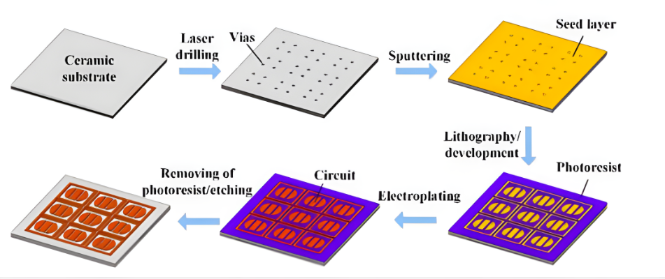
Physical vapor deposition is a low-temperature process (below 300℃), which completely avoids the adverse impact of high temperature on the material or line structure, and also reduces the cost of the manufacturing process, but the thickness of the electroplating deposited copper layer is limited, and the electroplating waste liquid pollution is large.
The above are several common methods for metallization of aluminum nitride ceramic substrates, and their respective advantages and disadvantages are shown in the table above. In addition to the above methods, fusion welding, solid phase diffusion, self-propagating high temperature synthesis and other methods can also be used for the metallization of aluminum nitride ceramic substrates.


